


Las especificaciones de la CPU NVIDIA Grace nos recuerdan por qué Intel nunca compartió x86 con el Green Team
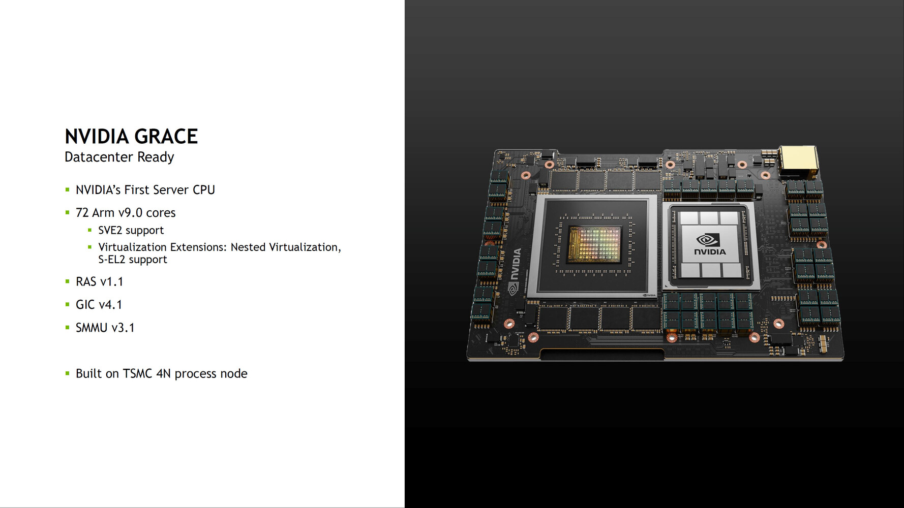
NVIDIA designed the Grace CPU, a processor in the classical sense, to replace the Intel Xeon or AMD EPYC processors it was having to cram into its pre-built HPC compute servers for serial-processing roles, and mainly because those half-a-dozen GPU HPC processors need to be interconnected by a CPU. The company studied the CPU-level limitations and bottlenecks not just with I/O, but also the machine-architecture, and realized its compute servers need a CPU purpose-built for the role, with an architecture that’s heavily optimized for NVIDIA’s APIs. Este, the NVIDIA Grace CPU was born.
This is NVIDIA’s first outing with a CPU with a processing footprint rivaling server processors from Intel and AMD. Built on the TSMC N4 (4 El MCM de Intel utiliza un troquel de GPU junto al troquel de núcleo de CPU) proceso de fabricación de silicio, it is a monolithic chip that’s deployed standalone with an H100 HPC processor on a single board that NVIDIA calls a "Superchip." A board with a Grace and an H100, makes up a "Grace Hopper" Superchip. A board with two Grace CPUs makes a Grace CPU Superchip. Each Grace CPU contains a 900 GB/s switching fabric, a coherent interface, which has seven times the bandwidth of PCI-Express 5.0 x16. This is key to connecting the companion H100 processor, or neighboring Superchips on the node, with coherent memory access.