


NVIDIA Grace CPU Specs Reminds Us Why Intel Never Shared x86 with the Green Team
NVIDIA designed the Grace CPU, a processor in the classical sense, to replace the Intel Xeon or AMD EPYC processors it was having to cram into its pre-built HPC compute servers for serial-processing roles, and mainly because those half-a-dozen GPU HPC processors need to be interconnected by a CPU. The company studied the CPU-level limitations and bottlenecks not just with I/O, but also the machine-architecture, and realized its compute servers need a CPU purpose-built for the role, with an architecture that’s heavily optimized for NVIDIA’s APIs. This, the NVIDIA Grace CPU was born.
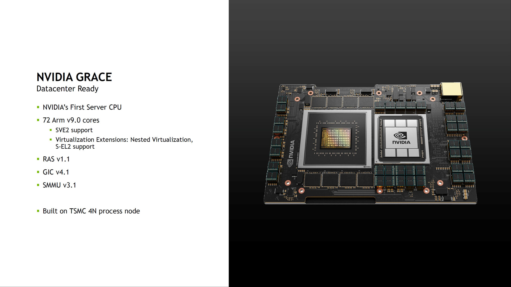
This is NVIDIA’s first outing with a CPU with a processing footprint rivaling server processors from Intel and AMD. Built on the TSMC N4 (4 nm EUV) silicon fabrication process, it is a monolithic chip that’s deployed standalone with an H100 HPC processor on a single board that NVIDIA calls a "Superchip." A board with a Grace and an H100, makes up a "Grace Hopper" Superchip. A board with two Grace CPUs makes a Grace CPU Superchip. Each Grace CPU contains a 900 GB/s switching fabric, a coherent interface, which has seven times the bandwidth of PCI-Express 5.0 x16. This is key to connecting the companion H100 processor, or neighboring Superchips on the node, with coherent memory access.